CS223 Laboratory Assignment 7
Arithmetic Logic Unit
Lab date and time:
- Section 1:
15.04.2010 08:40-12:30
Location: LAB 103 (in the new EEE building, next to and down
from the EA Building)
Groups: Each student should work with a partner in a 2-person group.
Important: There are some changes on the assigment as of 08.04.2010. Please make sure that you are working on the correct one.
Problem Description
In this lab assignment, you will design and implement a 3-bit Arithmetic Logic Unit (ALU) using the Xilinx ISE CAD tools, modeling it with Verilog. An ALU is an important part of a microprocessor, used to perform specified arithmetic and logic operations. ALUs have several functionalities, where the function to be performed is determined by the select inputs of the ALU. The ALU you will implement is specified below. The ALU model will be simulated using the ISim software, and downloaded into the Digilent FPGA board and tested, to verify correctness.
Specifications
The ALU can perform 8 different arithmetic or logic operations on two 3-bit operands. The schematic representation of the ALU is given in the figure. The inputs and the outputs are as follows:
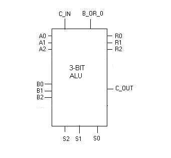
- A2, A1, A0: 3-bit unsigned integer operand A where A0 is the least significant digit.
- B2, B1, B0: 3-bit unsigned integer operand B where B0 is the least significant digit.
- C_IN: 1-bit carry-in/borrow-in that will be used for addition (as a carry) and subtraction (as a borrow). For these operations you CANNOT assume a particular value for C_IN. It should be taken as an input which can be either 0 or 1 for addition and can be 0 or 1 subtraction! The other six operations are performed without regard for this input.
- B_OR_0: Specifies whether the second operand is B or 0. (if 1, then second operand is B, else second operand is 3-bits of 0.)
- S2, S1, S0: the select bits which determine which ALU function to perform on the inputs.
- R2, R1, R0: 3-bit result R where R0 is the least significant digit.
- C_OUT: 1-bit carry-out that will be used for addition and subtraction.
The three select inputs will be used to select the operation that will be performed. The operations to be performed, for each configuration of select inputs, are as follows:
|
S2 |
S1 |
S0 |
Operation |
Result |
|
0 |
0 |
0 |
Subtract |
R=|A-B-C_IN| , C_OUT gives sign |
|
0 |
0 |
1 |
Add |
R=A+B+C_IN, C_OUT gives carry |
|
0 |
1 |
0 |
Rotate_Left |
R2=A1 R1=A0 R0=A2 |
|
0 |
1 |
1 |
Shift_Right |
R2=0 R1=A2 R0=A1 |
|
1 |
0 |
0 |
AND |
Ri=Ai AND Bi |
|
1 |
0 |
1 |
OR |
Ri=Ai OR Bi |
|
1 |
1 |
0 |
XOR |
Ri=Ai XOR Bi |
|
1 |
1 |
1 |
XNOR |
Ri=Ai XNOR Bi |
- Add: 3-bit adder with carry in C_IN, and carry out C_OUT
- Subtract: 3-bit magnitude subtractor with borrow in C_IN; R is the magnitude, of the difference, C_OUT =1 when the result is negative, 0 otherwise
- Rotate_Left: The input B will be ignored. Only the bits of A will be rotated left in a circular manner. That is R2=A1 R1=A0 R0=A2.
- Shift_Right: Similar to Rotation but the incoming bits will always be zero. The input B will be ignored. R2=0, R1=A2 and R2=A1.
- AND: Simple logical bit-wise AND operation performed individually on all bits. [That is Ri=Ai AND Bi, for all i.]
- OR: Simple logical bit-wise OR operation.
- XOR: Simple logical bit-wise XOR operation.
- XNOR: Simple logical bit-wise XNOR operation.
Advance Work (before lab)
Design the ALU circuit specified above. The design should be done in Verilog, as a module (or modules). Since there are various styles of Verilog modeling, you should consider which style is best for this assignment and write the program for your module(s) accordingly. Among your options are hierarchical and non-hierarchical models, structural, dataflow and behavioral styles, use of higher level constructs such a case and always, etc. CHECK YOUR DESIGN carefully, to increase your chance of success in the lab. You may even want to make several different designs, using some of the various Verilog styles, in order to see which will have the greater chance of working correctly. [Remember: research has consistently proven that the number of errors in software is in direct proportion to the size of the program.]
Before Lab:
0. Obtain a Digilent BASYS 2 board and install the Xilinx ISE 11 software to your personal laptop computer (see Lab 5 for details).
- Design the project, considering how you will model the ALU in Verilog. You may want to use hierarchical decomposition to obtain the components that will be needed in the overall solution. Then write the Verilog code for each of the components, making each a module. Assemble the modules in the hierarchy, to comprise the overall design. Using Xilinx ISE, make a project and add the Verilog source modules, and check for syntax and semantic errors.
- Test each of your Verilog modules individually, moving from modules low in the hierarchy upward to the top. Rather than physically download and test on the Digilent board, you should test using simulation, by creating a testbench within Xilinx. When the top-level module Lab7 is fully working, you are ready to create a user constraint file and download it to the Digilent board for manual verification. Using the switches as inputs, and the LEDs and 7-segment displays as outputs, test the circuit you have implemented and obtain the 11-input, 4-output results for important values of the functions you have built and verify that they perform the ALU functions specified above. For logic and shift functions, the outputs should be on the LEDs, but for arithmetic funtions, let the outputs display on two 7-segment displays, with the left-most one indicating a negative sign for negative results. [Note that you will need to use a pushbutton switch, to select which 7-segment display is activated.]
- When all is working with your design, write up the Preliminary Lab Report as described below.
Preliminary Lab Report (30 points):
You should prepare the Preliminary Report (as described below and in the Lab Policies) to be submitted at the start of lab. Make a copy for your own use during the lab, since the original will not be returned until after it is graded. The preliminary report should contain your Verilog program modules, together with any diagrams of blocks or structure that you have directly modeled.
At the start of lab, you should submit a Preliminary Lab Report, containing the following items, each starting at the top of a new page:
· Cover page, containing the course number and course name, the Lab number and lab name, the date, the names, ID numbers, and section numbers of each lab partner
· ALU function table
· Explanation of the design chosen, explaining why this particular approach was decided on. With this, you should give a block diagram (with internal structure shown) of all blocks in the design hierarchy. [Note: there should be one block for each Verilog module.]
- Verilog code for the overall module Lab7
- Verilog code for any other modules you create
The Verilog modules are code, and as with any program code, they should be well-structured, well-commented, use meaningful identifiers, use white space and indentation as appropriate to facilitate understanding, and in summary, should be self-documenting. If code is difficult to understand, it is not self-documenting!
All pages in the report, with the possible exception of a hand-drawn logic diagram, should be printed, front side only. All pages should be on white A4 paper. The pages in the package should be stapled together in the order given, attaching in the upper left-hand corner. The whole package should have a neat, clean, professional appearance.
You should come to lab fully prepared. Your Preliminary Lab Report will be submitted when you enter, so make a photocopy for yourselves, for your group to use during the lab. You should arrive with the problem above fully implemented and tested and ready to show to the TAs. When you arrive in lab, there will be a modification of the project specification written on the board for your section. You must implement this real-time in the lab, and show a working demo of it to the TA before the end of lab time.
Simulation of Circuit (30 points)
Implement the ALU you have designed using Verilog in a new Xilinx project and test it extensively. For each module that you write, create a Verilog Test Fixture and use it to simulate the behavior of the module with inputs of your choosing. [Actually, these tasks should already be done at home, before the start of lab.] When you are convinced that your overall Lab7 module works correctly under all possible input conditions, you should set up a simulation, to demo your project to the TA. Since the total simulation of your ALU under every possible input combination would take too long (11 inputs means 2^11 = 2048 input combinations), you should wisely choose a variety of inputs in all 8 modes of operation to use in demonstrating that your system works to specification. The test values should include boundary values, and other important values (e.g. that would cause carry, or with C_IN high and low, etc). When you are ready to be graded, show your simulation of the ALU with ISim to the TA. [You are required to order your input and output waveforms in the simulation window in such a way that the results for each input can be easily understood!]
Physical Circuit with FPGA (40 points)
a) You will be asked to create a new project in Xilinx, modifying your design (the new specification will be given to you in the lab), as proof that you understand what you are doing and can respond to changes in the specification real-time. This may involve changes in the Verilog, in the simulation testbench, in the User Constraint file, etc. You will show the TA your modified working circuit in the Digilent board, and the demo of your new project will be graded.
b) Finally, the TA will ask each lab partner questions to check your knowledge and understanding of the project and Verilog, and you will receive a grade according to your answers.
As a result, your grade and your partner’s grade might not be the same grade, depending on your answers to the oral questions.
Cleanup!
Clean up your lab station, and return all the parts, etc. If you used a lab computer, delete the Xilinx Project you created and any files you created today, so that the computer is in the same state that you found it. Now turn off the computer, and leave your lab workstation for others the way you would like to find it.
Notes
-- Be sure to read and follow the Policies for CS223 labs.
-- An extensive tutorial is posted online at http://www.cs.bilkent.edu.tr/~oonder/CS223/ . You will find that this written tutorial provides vital information on how to create a project in Xilinx 11 and how to download it into the Digilent BASYS 2 FPGA board.
-- The PCs in the lab contain the Xilinx and Digilent
software, installed, but these computers are extremely slow. You should use
your own laptop computer to develop, test, debug and make ready the project
before you come to the lab. On the day
of your lab, you will be much better off to bring your own laptop computer with
you, and to demonstrate the assignment using it. The idea is for your group to
be able to bring your fully tested, debugged and working systems to lab, only
to be graded.
-- Recommended reading: Mano & Kime textbook, Chapter 9 pages on ALU design, in sections 9-2 and 9-3. Notice that the authors give a hierarchical design, and implement it structurally. However, remember that you will be modeling in Verilog, and that other design styles are possible, and may even be better!
-- Your lab group must prepare a preliminary report before coming to lab. The report should have both students' names, ID numbers and the section of CS223 (1, 2, 3, or 4) that you are registered for in the upper right hand corner of each page. This report should include the ALU function table, a block diagram of the ALU, lower-level block diagrams if you implement it in a hierarchy of structures, and your Verilog code (all modules). We will collect these reports BEFORE the lab begins (35% of your grade will be based on this report). Since you will not have your original lab report during lab hours, you and your partner should make a photocopy of it before coming to lab, for your use in the lab.
-- As with all software code, your program should be well structured, well commented, and use meaningful labels to be self-documenting. Good style also suggests use of bold type (for reserved words), alignment and white spacing for easy readability. Besides these style features, your program should make good choices for modeling the ALU in an efficient way. You should seek to use the high-level features of the language whenever possible (see Verilog Resources page for more info).